To create the Arithmetic sub-block we will need to have a 32-bit adder with carry-in, carry-out, and overflow computation. Instead of going through the process of building this from scratch, we will be using an adder which has already been designed and instantiating it as a Component in our design.
You have already seen that the blue colored sub-blocks which you have placed in the ALU block diagram generate entity declarations with corresponding architectures created from their views which are then instantiated in the ALU architecture as components. In Renoir, however, these sub-blocks are not referred to as components because you cannot instantiate them in another design as they are; they are tied to one instance in one design. A sub-block can, however, be converted into a Renoir component, represented by a green colored box. They are essentially the same except for the fact that a component can be accessed from other design units to be instantiated.
Components allow for the creation of design libraries of commonly used objects which can be instantiated in new designs. I have created a 32-bit adder component and placed it in a library which will hold public design components that we will be using. Before we can use this adder in our ALU design, we will need to create a mapping to the new library.
The class design library will be called COELib and will be located at I:\1502\COELib. From the Design Browser, open the Library Mappings window from the Options menu. Left-click Add to bring up the Add Library Mapping window and fill in the appropriate data using the conventional subdirectories for source, hdl, and simulation data. When you are done, the window should look like Figure 1.
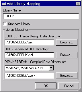
Figure 1
It is not necessary for a library to be open in the Design Manager in order to instantiate a component from it. In order to see what is in the library, though, go to the Open Library window from the File menu and open the COELib library. Expand the design tree in the source window to see a single design unit, in green, called Add32 with a symbol and single VHDL Architecture view called behav.vhd. The Design Manager window will look like Figure 2.
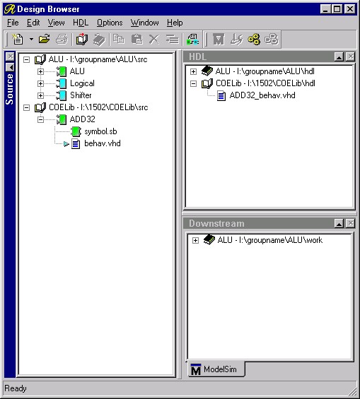
Figure 2
Now that we have mapped the COELib library, we can get started designing the Arithmetic unit. Open the ALU design from the Design Manager. Once you have done this, create a new block diagram view for the Arithmetic sub-block by right-clicking on the sub-block and selecting New View from the Open item on the pop-up menu. This will bring up the block diagram with ports seen in Figure 3.
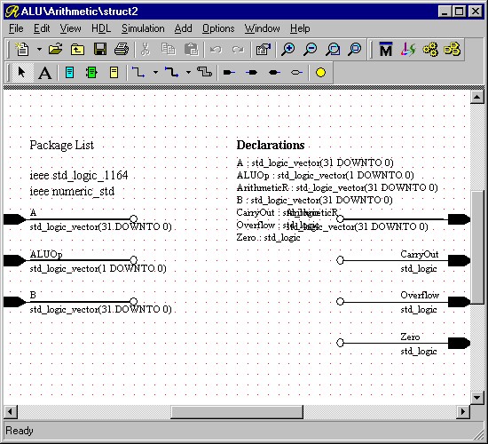
Figure 3
Now we wish to instantiate an add32 component. Activate the
Add Component tool by selecting the button,
 , from the toolbar. This
will bring up the Add Component window in Figure 4 which
will allow you to select which component to instantiate. In
the leftmost frame, select the COELib library. The
word COELib will appear in the box above this frame. In the
middle frame you will then see a list of the components in this
library, ADD32 will be the only one listed in this case.
Select the ADD32 component and ADD32 will appear
in the box above the middle frame. Also, since the View Type
setting in the lower right side is set to Default, the
box above the rightmost frame will be grayed out and the default
architecture for ADD32, which is behav.vhd, will be used.
Click OK when you have the proper component selected.
, from the toolbar. This
will bring up the Add Component window in Figure 4 which
will allow you to select which component to instantiate. In
the leftmost frame, select the COELib library. The
word COELib will appear in the box above this frame. In the
middle frame you will then see a list of the components in this
library, ADD32 will be the only one listed in this case.
Select the ADD32 component and ADD32 will appear
in the box above the middle frame. Also, since the View Type
setting in the lower right side is set to Default, the
box above the rightmost frame will be grayed out and the default
architecture for ADD32, which is behav.vhd, will be used.
Click OK when you have the proper component selected.
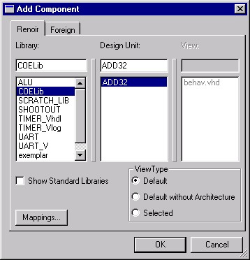
Figure 4
You will now see the message box in Figure 5 pop up asking whether you wish to add the package arithmetic.std_logic_arithmetic to your design. This is a VHDL package which is used in the adder. However, since there is nothing in the interface to the ADD32 component which requires this package (all ports in and out are in the std_logic_1164 package which is automatically declared) we do not need this package reference. Respond no to move on. You will now be see a shadow of the component as your pointer in the design area. Left-click somewhere in between the ports to place one instance of the component, then deactivate the tool.
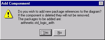
Figure 5
In addition to the ADD32 component, there are several other tasks which need to be accomplished: selecting B or NOT(B) and deciding whether to carry-in a '1' to configure for addition or subtraction; deciding whether or not to compute overflow; and calculating Zero which is high whenever the result is equal to zero and low otherwise.
These tasks will be implemented using Embedded Blocks just like in the Logical sub-block. We need to place three Embedded Blocks:
-
One we will call TOBORBNOT and will place to the left of the ADD32 component. This will perform two functions, one is to create an inverted version of B and the other is to assign B to the internal signal BTEMP when we are adding (when ALUOp(1) = '0') and assign the inverted version of B when we are subtracting (when ALUOp(1) = '1').
-
The second embedded block will pass the OFL output of the adder to the Overflow output when we are performing the ADD or SUB operations (ALUOp(0) = '0') and '0' otherwise. Place this block to the right of and below the ADD32 component and call it OVERFLOW.
-
The last embedded block will be placed to the right of the ADD32 component and will be called CALCZERO. Its primary function is to set the Zero output high when the adder result is equal to zero and set it low otherwise. This requires the block to "read" the result coming out of the ADD32 component. Since it is not possible to "read" values from output only ports, we cannot directly connect the result ArithmeticR to the output of the adder. We must instead create an internal signal which can be "read" to determine zero. Thus, as a second function, this embedded block will assign the value of the internal signal S to the output ArithmeticR.
After adding these blocks your block diagram should look like Figure 6.
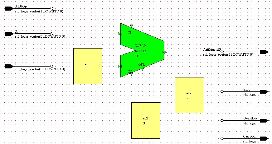
Figure 6
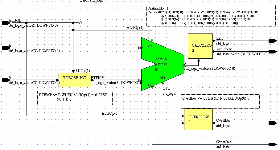
Now that the embedded blocks and the ADD32 component have been placed on the block diagram, connect the input and output ports and create the necessary internal signals so that the block diagram resembles Figure 7.
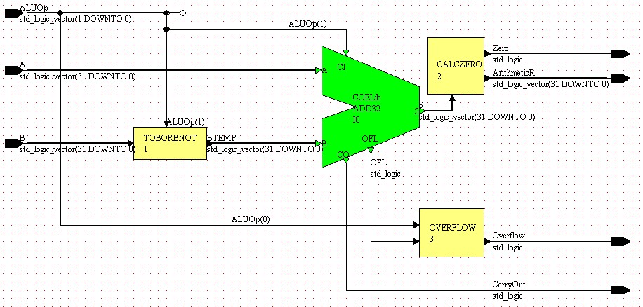
Figure 7
The final step, after all signals are connected properly is to define the behavior of the embedded blocks. The embedded VHDL text should be as follows:
-
TOBORBNOT :
		BTEMP <= B WHEN ALUOp(1) = '0' ELSE
		         NOT(B);
This embedded block implements a multiplexor with B as the input when the select, ALUOp(1), equals zero to implement and add and NOT(B) when the select equals one to implement a subtract. The other step necessary to implementing subtraction, carrying in a one, is taken care of by connecting ALUOp(1) to the carry-in of the adder. This way, when adding the carry-in is zero and when subtracting the carry-in is one.
-
OVERFLOW :
Overflow <= OFL AND NOT(ALUOp(0));When ALUOp(0) = '0' we want to perform arithmetic with overflow. When ALUOp(0) = '1', we want to perform arithmetic without overflow. Thus, by ANDing the overflow output of the adder, OFL, with the inverse of ALUOp(0), which is '1' if we want overflow output and '0' if we do not, we achieve the desired results.
-
CALCZERO :
		ArithmeticR <= S;
		Zero <= NOT(S(31) OR S(30) OR S(29) OR S(28) OR S(27) OR S(26) OR S(25) OR S(24) OR
		            S(23) OR S(22) OR S(21) OR S(20) OR S(19) OR S(18) OR S(17) OR S(16) OR
                        S(15) OR S(14) OR S(13) OR S(12) OR S(11) OR S(10) OR S(9) OR S(8) OR
		            S(7) OR S(6) OR S(5) OR S(4) OR S(3) OR S(2) OR S(1) OR S(0));
This block contains two VHDL statements, necessary because we cannot simultaneously assign the output of the adder directly to ArithmeticR and at the same time use that value to determine the Zero output. The first statement takes the internal value of the adder output, S, and assigns it to the result, ArithmeticR. The second statement determines whether the adder output is equal to zero by ORing the individual bits together. If the result of the OR is '0', meaning the result is zero, we want to output a '1' and if the result of the OR is a '1', meaning the result is non-zero, we want to output a '0'. Thus we invert the result of the OR to obtain our Zero output.